insulated gate bipolar transistor

CHAPTER 4: The Bipolar Transistor ppt
Ngày tải lên :
08/08/2014, 16:22
... OBJECTIVES Describe and Analyze: • Transistor architecture • Transistor characteristics • Transistors as switches • Transistor biasing • Transistor amplifiers • Troubleshooting techniques ... characteristic of a bipolar transistor is that a small amount of power in the base-emitter circuit can control a larger amount of power in the collector-emitter circuit
Inside the Transistor A small ... = 50 1mA = 50 mA Transistor Switches Compared to mechanical switches, transistors used as switches: • Last much longer • Can turn on and off much faster Calculations for a Transistor Switch...
- 19
- 239
- 0
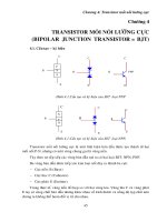
giao trinh linh kien dien tu CHUONG 4 TRANSISTOR MỐI NỐI LƯỠNG CỰC (BIPOLAR JUNCTION TRANSISTOR = BJT)
Ngày tải lên :
19/09/2013, 17:03
... 30A IB = 15A 50 IB= A VCE (v) Chương 4: Transistor mối nối lưỡng cực Hình 4.10 Họ đặc tuyến ngõ BJT 4.6 Hình dạng C 828 H 1061 Hình 4.11 Hình dạng loại transistor 4.7 Phân cực BJT BJT có nhiều ... Dòng từ cực E gọi dòng IE 4.3 Hệ thức liên quan dòng điện R R C E IC V EE IB IE VEE 46 Chương 4: Transistor mối nối lưỡng cực Hình 4.4 Sự dòch chuyển điện tử cho thấy: IE = IB+IC (1) IC = IE (2) ... CB0 IB IC α I CB0 1 α IC IB α α IC = I α I B CB0 1 α 1 α 47 Chương 4: Transistor mối nối lưỡng cực IC = IB + I CB0 (7) 1 α Khi bỏ qua dòng điện rỉ ICB0 phương trình...
- 20
- 1.1K
- 18
Chapter 2 characteristics of bipolar junction transistor
Ngày tải lên :
12/05/2014, 23:16
... CHAPTER 2: Characteristics of Bipolar Junction Transistor CHAPTER 2: CHARACTERISTICS OF BIPOLAR JUNCTION TRANSISTOR 2.1 BJT CONSTRUCTION AND SYMBOLS The bipolar junction transistor (BJT) is a three-element ... Characteristics of Bipolar Junction Transistor Table 2-1 Notation for voltages and currents 2.2 COMMON-EMITTER TERMINAL CHARACTERISTICS The common-emitter (CE) connection is a two-port transistor arrangement ... Characteristics of Bipolar Junction Transistor Table 2-2 Operating modes Saturation denotes operation (with vCE 0.2V and vCB 0.5V for Si devices) such that maximum collector current flows and the transistor...
- 9
- 387
- 0
Điện tử học : Transistor lưỡng cực nối (Bipolar junction Transistor) part 5 docx
Ngày tải lên :
26/07/2014, 20:21
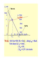
... Vai trò đường thẳng tải tĩnh • Phân giải mạch Transistor • Xác định điểm tĩnh điều hành Q • Cho biết trạng thái hoạt động cũa transistor ( tác động, bão hồ, ngưng) • Mạch khuếch đại ... đổi theo vị trí điểm tĩnh điều hành Q • Điểm tĩnh điều hành Q thay đổi vị trí theo điện phân cực transistor thay đổi theo tín hiệu xoay chiều ( AC) tác động vào mạch • Ta xét dạng mạch phân cực ... dòng • Theo hình ta có: • IC = mA IB = 40 A • Tính độ lợi dòng : I CQ 4mA 100 I BQ 4 A o Transistor có tính khuếch đại dòng o Độ lợi dòng tính nhanh từ đồ thò • Độ lợi dòng chế độ động...
- 6
- 377
- 0


Điện tử học : Transistor lưỡng cực nối (Bipolar junction Transistor) part 3 doc
Ngày tải lên :
26/07/2014, 20:21
... Chú ý :Transistor gọi là: linh kiện điều khiển băng dòng điện linh kiện điều khiển hạt tải thiểu số TRANSISTOR chử viết tắt từ TRANSfert resISTOR (Điện trở chuyển ) 4.Đối với transistor loại ... cách lý luận hoạt động giống transistor npn thay đttd lổ trống, nên chiều dòng điện ngược lại
III.Các cách ráp Đặc tuyến V-I • Có cách ráp (xác định từ ngõ vào ngõ mạch transistor) : CB, CE, CC...
- 6
- 314
- 0

Điện tử học : Transistor lưỡng cực nối (Bipolar junction Transistor) part 2 ppsx
Ngày tải lên :
26/07/2014, 20:21
... trừ IC số cấu trúc đối xứng nên cực thu C cực phát E thay vị trí cho Chú ý: 1.Trong phần khảo sát transistor hoạt động khuếch đại ta xét đến kiểu tác động (BE phân cực thuận, CB phân cực nghịch)...
- 6
- 270
- 0

Điện tử học : Transistor lưỡng cực nối (Bipolar junction Transistor) part 1 pptx
Ngày tải lên :
26/07/2014, 20:21
... I Cấu tạo • Gồm nối tiếp xúc ghép xen kẽ • Có loại Transistor nối: npn pnp (h 1) • C C n • • C p B B C B B • p n • n p • E loại npn E E loại pnp E...
- 6
- 309
- 2

Bipolar Junction Transistor (BJT)
Ngày tải lên :
30/05/2015, 11:45
... Troubleshooting Transistors (Transfer Resistor) Transistors Bipolar transistors NPN,PNP Field Effect Transistors Junction-FETs (JFETS) N-channel, P-channel Insulated Gate FET’s MOSFETs Enhancement, Depletion ... dung chương 6 Transistor chưa phân cực Transistor có phân cực Các dòng điện transistor Mắc E chung (CE) Đặc tuyến cực Đặc tuyến cực thu Xấp xỉ transistor Đọc bảng liệu Troubleshooting Transistors ... Từ Vựng (1) • • • • • • • • • Active region = miền tích cực Base (B) = (miền/cực) Bipolar transistor = transistor lưỡng cực Breakdwon region = miền đánh thủng Collector (C) = (miền/cực) thu...
- 77
- 1.2K
- 0

Strained multiple gate transistors with si sic and si sige heterojunctions
Ngày tải lên :
11/09/2015, 16:07
... Background 1.2.1 Multiple -Gate Transistors Multiple -gate FETs provide better electrostatic control than single -gate FETs [1.13] An example of the multiple -gate transistor is the double -gate (DG) FET A ... gate dielectric Poly-Si gate material was then deposited Gate implant was performed and activated A SiO2 hardmask was then deposited After gate patterning, photoresist trimming and etching, gate ... multiple -gate transistors must also be developed In this thesis, strain engineering techniques using lattice-mismatched source and drain stressors for both n and p-channel multiple -gate transistors...
- 192
- 151
- 0
Schottky source drain transistor integrated with high k and metal gate for sub tenth nm technology
Ngày tải lên :
14/09/2015, 14:04
... of either the gate dielectric capacitance density Cinv or the channel carrier mobility µ , or both of them 1.2 High-k gate dielectrics and metal gate The MOS gate structure in a transistor (see ... the poly-Si gate, thus can be eliminated by replacing poly-Si gate with metal gate One of the most widely studied metal gate materials, Tantalum Nitride (TaN), was used as metal gate in this ... to diode Vg Voltage applied to the transistor gate Vth Threshold voltage of transistor Vr Reverse voltage bias to diode VFB Flatband voltage W Width of the transistor channel XPS X-ray photoelectron...
- 146
- 810
- 0

Threshold voltage instabilities in MOS transistors with advanced gate dielectrics
Ngày tải lên :
14/09/2015, 14:04
... NAND3 gate implemented with static logic, b) 2-input multiplexer implemented with CMOS transmission gate, and c) NAND3 gate implemented with dynamic logic 115 4.23 Percentage increase in gate ... positive supply voltage Vds drain-to-source voltage Vfb flat-band voltage Vg gate voltage Vgd gate- to-drain voltage Vgs gate- to-source voltage Vmeas measurement voltage Vout output voltage Vstress ... concerning transistor technology, the 60th anniversary of the invention of transistor (23rd, December 1947) is approaching It is interesting to note that, though the first practical transistor, ...
- 150
- 250
- 0

Advanced source and drain contact engineering for multiple gate transistors
Ngày tải lên :
15/09/2015, 21:48
... image of the transistor showing a conformal growth of Si1-yCy on the S/D regions with the revmoval of the SiN stringers (c) Cross sectional TEM showing a transistor gate stack with a gate length ... representation of a triple -gate structure with the gate electrode encompassing the three sidewalls of the silicon fin to form the device channel The term “double gate refers to a single gate electrode that ... on two opposite sides of the transistor channel Similarly, the term “triple -gate is used for a single gate electrode that is encompassing over three sides of the transistor channel Figure 1.1...
- 191
- 300
- 0

Characterization and numerical simulation of gallium nitride based metal oxide semiconductor high electron mobility transistor with high k gate stack
Ngày tải lên :
03/10/2015, 20:31
... 21 b) a) Gate Gate Width Drain Source Figure 3.1 a) A typical transistor design for the purpose of DC characterisation W, L and LD-G referred to the gate width, gate length and drain -gate separation ... Electron Mobility Transistor 20 Figure 3.1 a) A typical transistor design for the purpose of DC characterisation W, L and LD-G referred to the gate width, gate length and drain -gate separation ... resistance of the device 3.1.2 Source -Gate/ Drain -Gate Separation Apart from having a variety of devices with different gate dimensions such as gate length and gate width, one of the factors that...
- 142
- 446
- 0
Characterization and numerical simulation of gallium nitride based metal oxide semiconductor high electron mobility transistor with high k gate stack
Ngày tải lên :
12/10/2015, 17:36
... 21 b) a) Gate Gate Width Drain Source Figure 3.1 a) A typical transistor design for the purpose of DC characterisation W, L and LD-G referred to the gate width, gate length and drain -gate separation ... Electron Mobility Transistor 20 Figure 3.1 a) A typical transistor design for the purpose of DC characterisation W, L and LD-G referred to the gate width, gate length and drain -gate separation ... resistance of the device 3.1.2 Source -Gate/ Drain -Gate Separation Apart from having a variety of devices with different gate dimensions such as gate length and gate width, one of the factors that...
- 142
- 925
- 0

Transitor lưỡng cực (bipolar junction transistor BJT)
Ngày tải lên :
31/12/2015, 17:09
... nên ta coi như: IE # IC 2/21 Transitor lưỡng cực (Bipolar junction transistor - BJT) CÁC CÁCH RÁP TRANSISTOR VÀ ĐỘ LỢI DỊNG ĐIỆN Khi sử dụng, transistor ráp theo cách sau: • Ráp theo kiểu cực ... nhiệt độ ảnh hưởng quan 8/21 Transitor lưỡng cực (Bipolar junction transistor - BJT) trọng đến điểm điều hành transistor Nó ngun nhân làm cho thơng số transistor thay đổi kết tín hiệu bị biến dạng ... IE 12/21 Transitor lưỡng cực (Bipolar junction transistor - BJT) Áp dụng định luật kirchoff (ngõ ra), ta có: • Với transistor NPN: VCB = VCC - RC.IC; VCB > • Với transistor PNP: VCB = -VCC + RC.IC;...
- 21
- 570
- 3

Transistor lưỡng cực Bipolar Junction Transistor, Nguyễn Quốc Cường , Đại học BKHN
Ngày tải lên :
05/07/2016, 19:05
... thiết bị truyền tin không dây Transistor lưỡng cực Nguyễn Quốc Cường Cấu trúc đơn giản BJT kiểu npn Transistor lưỡng cực Nguyễn Quốc Cường Cấu trúc đơn giản BJT kiểu pnp Transistor lưỡng cực Nguyễn ... tiếp giáp BJT có chế độ hoạt động khác Transistor lưỡng cực Nguyễn Quốc Cường Chế độ hoạt động BJT Transistor lưỡng cực Nguyễn Quốc Cường Chế độ tích cực Transistor lưỡng cực Nguyễn Quốc Cường ... RiSC Mô hình EM npn 10 Transistor lưỡng cực Nguyễn Quốc Cường Transistor pnp • Hoạt động pnp tương tự npn, có điểm khác biệt dòng điện chủ yếu tạo lên lỗ trống từ E đến B 11 Transistor lưỡng cực...
- 21
- 417
- 0

Transistor hiệu ứng trường FET Phần 1.pdf
Ngày tải lên :
20/08/2012, 11:16
... 6.1 Giới thiệu Transistor hiệu ứng trường (Field Effect Transistor – FET): JFET: Junction FET MOSFET: Metal-Oxid Semiconductor FET (Insulated- Gate – IGFET) Tính chất (Phân biệt ... iD : D → S: Phụ thuộc vào vDS Điện trở kênh n (Rn-Channel) Dòng iChannel – Gate ≈ 0: Do Diode tạo tiếp xúc pn Channel -Gate phân cực nghòch (a) Khi vDS tăng: Vùng khuyết (depletion region – vùng ... Vpo tăng Chương ⇒ “Voltage-Sensitive Device” Đồ thò: Lưu ý: n-JFET: Phân cực cho dòng IChannel -Gate (vGS ≤ vGS nhỏ > 0) 6.2.3 Đặc tuyến: Điện áp vDS điểm nghẽn: vDS-Pinch Off = Vp = Vpo + vGS...
- 13
- 2.3K
- 23
Tìm thêm:
- hệ việt nam nhật bản và sức hấp dẫn của tiếng nhật tại việt nam
- xác định các mục tiêu của chương trình
- xác định các nguyên tắc biên soạn
- khảo sát các chuẩn giảng dạy tiếng nhật từ góc độ lí thuyết và thực tiễn
- khảo sát chương trình đào tạo của các đơn vị đào tạo tại nhật bản
- khảo sát chương trình đào tạo gắn với các giáo trình cụ thể
- xác định thời lượng học về mặt lí thuyết và thực tế
- tiến hành xây dựng chương trình đào tạo dành cho đối tượng không chuyên ngữ tại việt nam
- điều tra đối với đối tượng giảng viên và đối tượng quản lí
- điều tra với đối tượng sinh viên học tiếng nhật không chuyên ngữ1
- khảo sát thực tế giảng dạy tiếng nhật không chuyên ngữ tại việt nam
- khảo sát các chương trình đào tạo theo những bộ giáo trình tiêu biểu
- nội dung cụ thể cho từng kĩ năng ở từng cấp độ
- xác định mức độ đáp ứng về văn hoá và chuyên môn trong ct
- phát huy những thành tựu công nghệ mới nhất được áp dụng vào công tác dạy và học ngoại ngữ
- mở máy động cơ lồng sóc
- mở máy động cơ rôto dây quấn
- các đặc tính của động cơ điện không đồng bộ
- hệ số công suất cosp fi p2
- đặc tuyến hiệu suất h fi p2